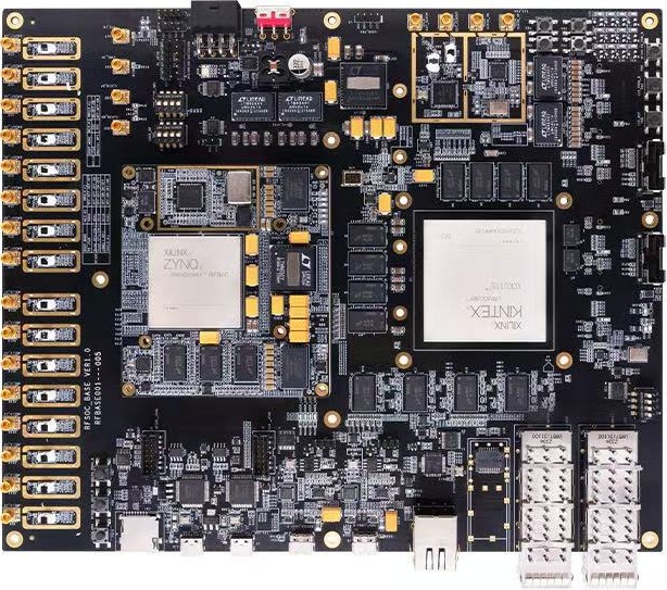
On a single board sit two large FPGAs: a Zynq UltraScale+ RFSoC that hosts the radio, and a Kintex UltraScale, joined by eight high-speed serial lanes. Neither chip alone had the room this design needed, so we turned the second chip into an extension of the first: a place to run extra logic, and four gigabytes of DDR4 beside it to use as remote memory, all reachable over the link. An AI did the hands-on work in our Python2Verilog framework; an engineer set the direction at each step.
The link: eight lanes, ten gigabits each
Each lane is two differential pairs, one for each direction, and eight are wired between the two chips. Every lane runs a 64B/66B block code: each 64 bits of data carry a 2-bit sync header, and the receiver locks once it sees enough legal headers in a row. The transceivers are rated into the tens of gigabits per second and here run near ten. One lane carries real bytes both ways, byte-exact. Bonding lanes into one wider channel is the way to widen it: a two-lane bond passes its own byte-exact gate, and the full multi-lane bond is still being closed, with one return path still parked on the board. So the eight lanes are physical provisioning, and the working link today runs on one. Getting that one direction to carry real bytes took a hunt, told below.
A link protocol we own
The first attempt used the FPGA vendor's own high-speed link. On this board it failed, for measured reasons: the reversed wiring forced the link into modes that never completed, defect stacked on defect. So the link runs a protocol we wrote ourselves, on the same 64B/66B block coding but with our own framing. It is deliberately thin. A small set of block types carries the stream, and block-lock is link-up. There is no training handshake, no credits, no link-layer checksum or acknowledgement. Each direction stands alone, and either side can join at any time.
The reason to own the link is physical and permanent. Each lane is electrically full-duplex, so the trouble is not direction but order: on this carrier the eight lanes run in reversed order in the copper, the Kintex transceiver channels 0 to 3 landing on the lane nets labelled 7 down to 4 while the RFSoC side counts up, so the RFSoC's lane i meets the Kintex's lane 7 minus i. The vendor link bonds lane N to lane N and needs a consistent, expected lane order to deskew and lock, so with the order mirrored the bonding never completes: each lane reaches block-lock on its own, yet the channel never reaches channel-up and the duplex link never comes up. A simplex fallback then hit a separate limitation of that vendor link on the Kintex transceivers, and that was the point to stop. Our own link never bonds lanes and carries its own framing, so a reversed lane order simply does not matter to it. It is also why the reversed record earlier was so costly: the reversal is a permanent fact of the copper, not merely a mistaken table.
Data and control share the one stream. Memory frames read and write the remote DDR4 byte-exact, and control frames carry a register read or write, a link re-init, status counters, even a warm reboot of the second chip over the link with no JTAG cable attached. Compute needs no opcode at all. The Wi-Fi decoder sits inline between the link's receive and transmit, so an arriving frame is its input and the decoded result is framed straight back.
Reliability is minimal on purpose. Block-lock recovers itself, the stream carries backpressure across an asynchronous clock-crossing buffer, and memory writes wait on their response. There is no checksum and no retransmit, because at this reach the byte-exact results show it does not need them. A single lane sustains about 3.0 gigabits per second, byte-exact, and over that same link we shipped the second chip its configuration and an 8.56-megabyte boot image, byte-exact, after which it rebooted itself from flash with no JTAG.
Four gigabytes of memory, pulled from a 75-page PDF
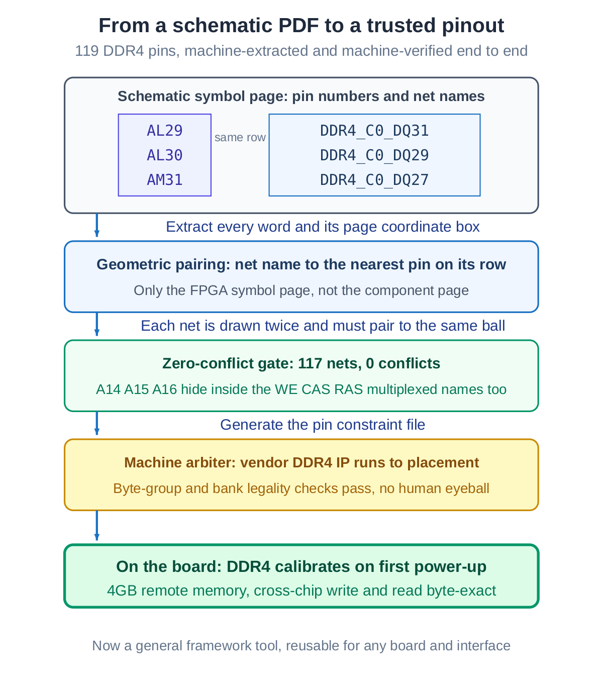
The four gigabytes of DDR4 beside the second chip had no machine-readable pinout, only a 75-page schematic PDF, and its 64-bit interface has 119 pins where one hand-copied wire means a failed calibration. So the AI turned it into a geometry problem: extract every word on every page with its coordinate box, pair each net name with the nearest pin number on the same row, and require every net to pair twice to the same pin or the whole thing is rejected. That zero-conflict gate resolved 117 nets with no conflicts, including the address lines hidden inside multiplexed names. The vendor's memory-controller IP was the arbiter: it ran to placement and passed its own byte-group and bank legality checks, with no human eyeballing a schematic. Burned to the board, the DDR4 calibrated on the first power-up.
The second chip becomes three things at once
With the link carrying real bytes and the memory calibrated, the second chip took on three roles, each proven on the real hardware. A 256-kilobyte round trip over the link came back byte-exact. A Wi-Fi LDPC decoder placed on the second chip took in 1,296 bytes of soft information and returned 164 bytes of decisions with zero errors against the reference model, and still zero errors when run twice without a reset in between. A four-kilobyte write across the link and back read out byte-exact, and again at a deep address. From then on the second chip is three things to the first: a byte-exact link, a compute node, and four gigabytes of remote memory.
One record fooled every check
Getting that link to carry real bytes both ways was the hard part, and it hid in the one place nothing measures. One direction came up quickly. The other kept sliding, always a hair short of lock, with no error and no crash. So we measured, layer by layer, and every layer passed: the vendor's own example simulation built the link; a loopback simulation carried a frame bit-exact; a cross-chip simulation wired to the real connection looped back byte-exact; an analysis of 400,000 bits on the simulated wire found the sync headers 100% legal at the one correct offset; and a comparison of the placed-and-routed netlists, pin by pin, found the good and bad builds identical. A scan of the receiver showed an eye wide open and clean, 77.8% horizontal and 93.6% vertical. The signal was flawless. The problem was not the signal.
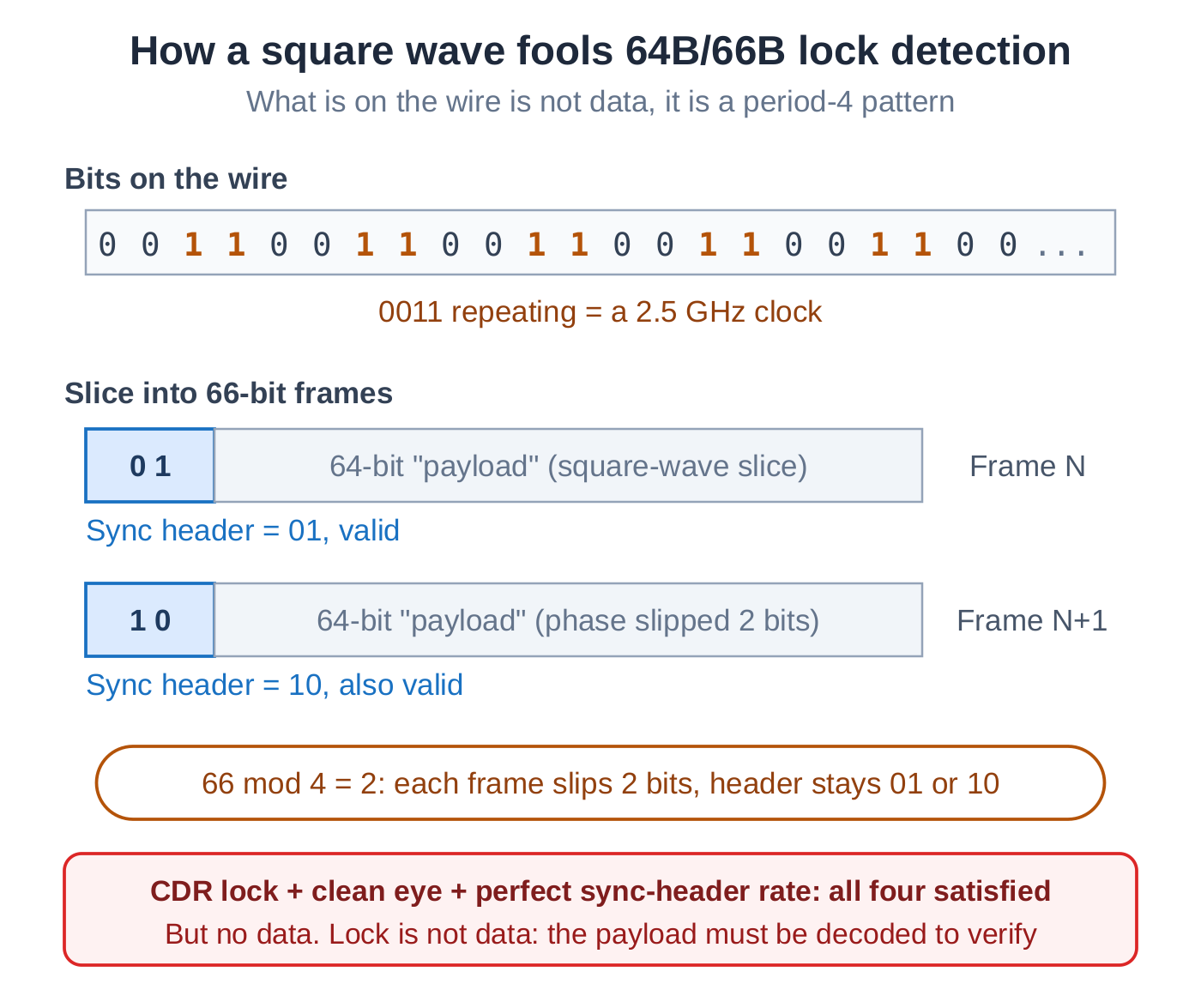
Every reading so far was a statistic. So we added a one-shot capture that read three consecutive raw 64-bit words straight off the locked lane. They came back as a repeating 0011 pattern, a plain square wave, a free-running clock. Scrambled data should look random; this carried no data at all. And 66 divides by 4 with a remainder of 2, so slicing the wire into 66-bit frames slides the phase by 2 bits each frame and the sync header always lands on 01 or 10, both legal. A clock had been impersonating a healthy link the whole time.
So we measured the lane wiring again, from scratch, by physical name rather than tool index, sending a different binary-coded marker down each lane. Three rounds resolved all eight, and the result was the exact opposite of the record we had been trusting. The transmitter had been sending correct data down a lane nobody was listening to, and the monitored lane was connected to one that had never been configured, free-running that square wave. Every simulation had wired itself from the same record, the record was internally consistent, so every simulation passed.
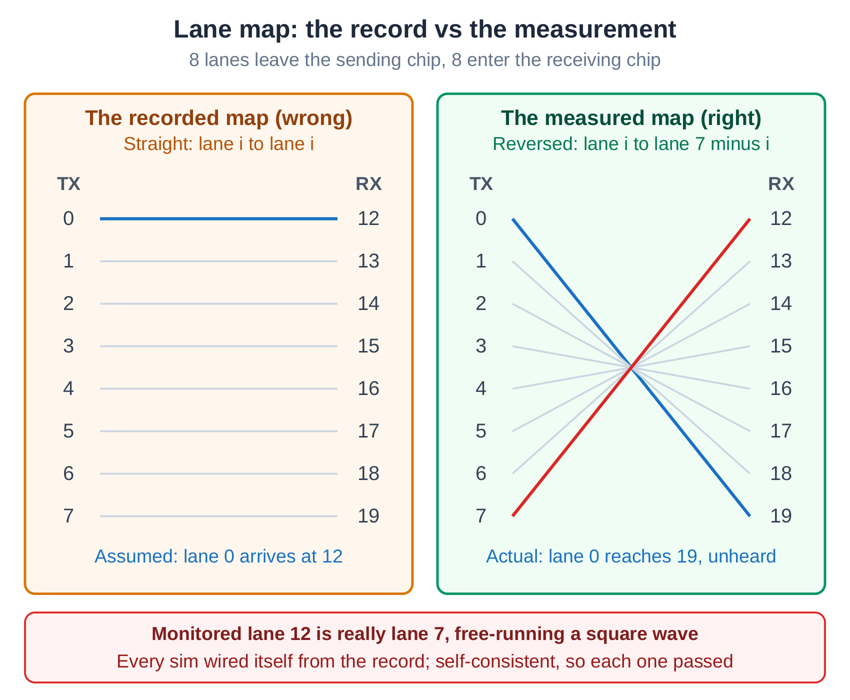
An earlier bit-error-rate test had run on these eight lanes, seven of them with zero errors, so it is fair to ask how it missed a reversed pair. That test sends the same pseudo-random sequence down every lane: whatever connects to whatever, each receiver locks and reports zero errors. It is blind by construction to which lane connects to which. The copper was fine on every lane. What was wrong was the table of which one went where. The fix was to rebuild on the two correct lanes, and it linked on the first try, byte-exact. Three genuine bugs found along the way were kept, but none was the cause. One loose end remained: the earlier test had flagged a trace of errors on one lane, the very lane the reverse link had used, so that lane was soaked on its own for ten minutes. Six trillion bits, zero errors, an eye as open as the other seven.
Three rules we kept
Each of these went back into the framework as a check that now runs on every build.
Lock is not data. A square wave can satisfy sync-header lock, CDR lock, a clean eye, and a perfect header-legality rate all at once. A link is only accepted when it decodes real payload and matches byte for byte.
A map is trusted only by physical name. Lane wiring is recorded by the physical names on both ends and measured with a distinct marker per lane. A tool's numbering is not evidence of what connects to what.
A pinout is trusted only by machine. Schematic pins are extracted by geometric pairing, admitted only when every net resolves with zero conflict, and validated by the vendor IP rather than by reading the drawing.
Why this matters
A second FPGA became a proven extension of the first: a 10-gigabit pipe, a compute node, and four gigabytes of remote memory, each verified byte-exact on the real board. What made that possible was the same discipline throughout. Prove each layer against a real reading, and trust the state of the hardware over the document that describes it. The one record with a reversed line survived a full day of work precisely because every simulation dutifully wired itself from it, and the fix was to measure the wire, not re-read the record. That is how the system came together, one measured step at a time.